Delving into the realm of Printed Circuit Board (PCB) manufacturing, one might be astounded by the intricacy and precision required at every stage. From the initial concept to the final circuit, understanding the process involves demystifying complex design strategies, decoding the manufacturing steps, and apprehending the significant role of components and layers in the assembly. This article sheds light on these aspects, highlighting the importance of the designer’s skillset, the impact of material selection, and the role of technology in modern PCB production.
Unraveling the Intricacies of PCB Design
Embracing the complexity of PCB design necessitates a deep understanding of the entire manufacturing process. A detailed ebook that elucidates the process of manufacturing a PCB, including design, layout, and common electrical issues is a valuable resource. It provides a comprehensive understanding of the role of electrical layout in PCB design. The layout, a critical aspect of PCB design, is effectively the blueprint of the circuit. It dictates the placement of components and the routing of electrical connections, thus directly impacting the performance of the final product.
Role of Electrical Layout in PCB Design
The layout, in essence, determines how the printed circuit board functions. An efficient layout ensures that electrical current paths are optimized, reducing the risk of potential issues such as signal interference and power dissipation. Moreover, a series of short videos offering expert advice on how to enhance the efficiency of PCB layout design are valuable assets for those looking to improve their skills.
Significance of Material Selection in PCB Design
Material selection plays a significant role in PCB design. The choice of substrate material, for instance, can greatly affect the electrical performance and durability of the PCB. A regular newsletter highlighting the latest trends and technologies in PCB design could provide updates on novel materials and techniques that could revolutionize the industry.
Impact of Designer’s Competence on PCB Design
The competence of the designer greatly impacts the effectiveness of the PCB. An interactive webinar where participants can learn and question about common mistakes in PCB design and how to avoid them is an excellent platform for designers to enhance their skills. Additionally, an organized list of recommended learning resources for those wishing to deepen their knowledge in PCB design is a valuable tool in the continuous learning process.
Decoding the Step-by-Step PCB Manufacturing Process
Starting with the conceptualization of the PCB design, the manufacturing process of a Printed Circuit Board (PCB) is a meticulous task that involves multiple detailed stages. The first stage comprises of the preparation of the board material, which is essential for the overall functionality of the PCB. The materials used play a critical role in the fabrication of PCBs, as they determine the performance and durability of the end product.
The PCB fabrication process involves various complex steps including etching and plating. Etching, a vital part of the PCB manufacturing process, involves the use of chemicals to remove unwanted copper from the circuit board. This process results in the formation of the desired circuit pattern. Plating, on the other hand, fortifies the copper that forms the circuits, thereby enhancing their conductivity and resistance to wear.
Once the circuits are formed, the PCB undergoes rigorous testing and inspection. This ensures that the PCBs meet the set quality standards before they are dispatched for assembly. These standards are put in place to ascertain that the PCB performs effectively in its intended application.
Understanding the PCB manufacturing process helps in appreciating the effort that goes into creating these essential components of almost every electronic device. The following points provide further details on the PCB manufacturing process:
-
The preparation of the board material is the initial step in the PCB fabrication process. The material selected for the board determines the functionality and durability of the PCB.
-
The etching process uses chemicals to remove unwanted copper from the circuit board, resulting in the desired circuit pattern.
-
Plating is used to reinforce the circuits, making them more conductive and resistant to wear.
-
Thorough testing and inspection ensure that the PCBs meet the necessary quality standards before being dispatched for assembly.
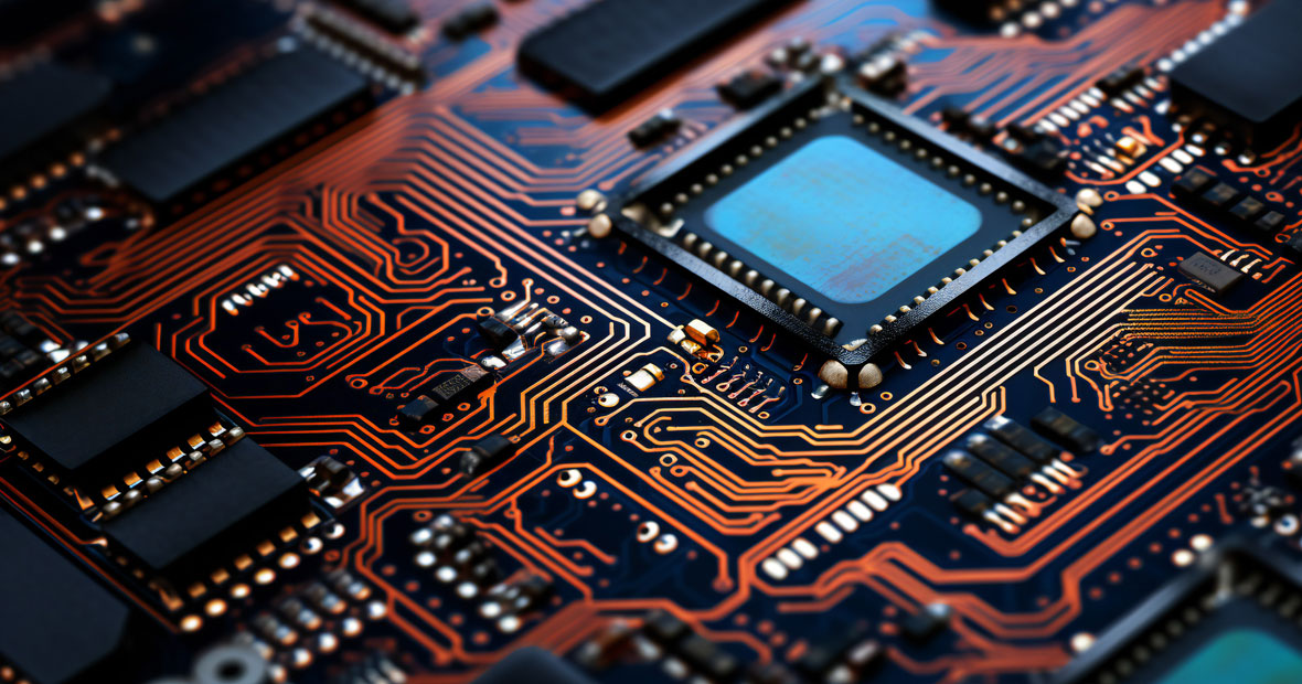
Insight into the Role of Components and Layers in PCB Assembly
For every intricate electronic device, a well-structured Printed Circuit Board (PCB) lays the foundation. The PCBs manufacturing process plays a significant role in the functionality and reliability of these devices. The process includes several stages from concept to circuit, with each stage playing a critical role in the overall performance of the final product.
Significance of Component Placement in PCB Assembly
In the stage of assembly, each individual component holds a pivotal role. Components are the integral parts of a circuit, with each having a unique function. The placement of these parts and their integration into the board is key to the successful assembly of PCBs. Misaligned or incorrectly placed components can lead to functionality issues, thus affecting the overall performance of the device. Therefore, utmost precision is required in component placement.
Role of Layers in Ensuring High-quality PCBs
PCBs are typically made up of multiple layers, including the inner and outer layers. Each layer has a specific role and is critical to the overall board design and functionality. For instance, the inner layers often contain the circuitry interconnecting the components, while the outer layers provide a protective coating. To ensure a high-quality final product, each layer must be accurately designed and implemented.
Understanding Soldering and its Role in PCB Assembly
Soldering, a vital process in the assembly of PCBs, involves the use of solder to connect the components to the surface of the board. A detailed tutorial video showing the soldering process can provide a clearer understanding of its role in the assembly of PCBs. It must be noted that the quality and type of solder used can significantly impact the connectivity and longevity of the board.
Exploring the Impact of Technological Advancements on PCB Production
Advancements in technological realms have significantly transformed the PCB production process. Traditional methods have given way to more sophisticated techniques, enhancing the speed, efficiency, and accuracy of PCB manufacturing. The emergence of modern machinery has revolutionized the creation of intricate electronic circuits, leading to the production of high-performance PCBs.
One notable change includes the use of Automated Optical Inspection (AOI) systems. These advanced machines inspect every aspect of the board, detecting and correcting any flaws in the manufacturing process. This ensures the final product meets the highest standards of quality and performance.
Another significant technological advancement is the photoengraving process, which uses ultraviolet light and photoresist film to create a copper layout on the PCB. In addition, the introduction of laser drilling machines has made it possible to create smaller and more precise holes, enabling manufacturers to produce more compact and complex PCBs.
These technological advancements have not only transformed the PCB production process but also broadened the scope for electronic device manufacturers. As a result, PCBs can now be used in a wider range of applications, from simple electronic devices to high-tech machinery and equipment.
Despite these technological advancements, selecting the right PCB manufacturer remains critical. Factors such as the manufacturer’s technological capabilities, quality standards, and production capacity should be considered to ensure the best outcomes.
Understanding the PCB manufacturing process and the impact of technological advancements is essential for anyone involved in the electronics industry. It helps in making informed decisions and staying competitive in a rapidly evolving industry.